
Building a MARK-8 mini computer replica (PCB’s and more available see below)
I am always interested in the technique used in old computers (or Vintage computers as the are called nowadays) and that’s why I have a small collection of vintage computers (about 100 machines I believe) from the early eighties. There was a time everyone threw them away and you could get them for a small amount of money. Today they are much more difficult to get for a reasonable price. Especially if you want to own the so called hobby computers from the seventies of the past century. But I also like to build computers from the ground up so when I visited the well documented website from Bryan Blackburn about the Mark 8 mini computer from 1974, publicized in Radio Electronics magazine July 1974 all designed by Jon Titus, I knew what to do. I was going to build one from scratch just for the fun of it.

At the end of this page you will find downloadlinks for all documentation I used.
But before I started spending a lot of time to design my own PCB’s I had to obtain all the needed components first. Where they still available? If I was going to build one I would like it to have all the original components and no substitute solutions for hard to find parts. It had to be an exact replica of the original, technical speaking that is. The cosmetic looks of the MARK-8 are not set in gold because it was a computer design which you had to build yourself and you could choose your own looks.
Most of the times these old designs use components which are obsolete and difficult to get hold off. When I looked at the components list I noticed that most (but not all) Integrated Circuits (I.C’s) where from the 74 TTL family which are still available. Although the MARK-8 used for example the 7400 where today you can only obtain the 74LS00 (LS-Low-power Schottky) version in an easy way. But that is no problem you can also use the LS type instead of the type without the letters in between.

MARK-8 minicomputer hard to find parts
The difficult to get parts where:
- 8008 CPU 1x needed
- 8263 Digital multiplexer 2x needed
- 8267 Digital multiplexer 2x needed
- 1101A1 256×1 Memory circuits 32x needed for just 1K (1024 bytes) memory, yes really!
After some searching I found the 8008 CPU and the Multiplexer on Ebay. The 8008 and the multiplexers where not cheap, they set me back about € 150,- but maybe you can do better ;-).

MARK-8 minicomputer 1101 memory IC’s
The Memory I.C.‘s where more difficult to get but I did find a company who still had a big stock of them so I bought a bunch for around € 3,- each. To pay almost €100 (32 x €3,-) seems a lot for just 1K of memory. I could use a more modern I.C. and make a more simple RAM PCB but that would be no exact technical replica of the original. If you want to reduce costs you can also only fill the first bank of the RAM board for 256 Bytes so you just need 8 pieces of 1101 Memory I.C.’s to make a working MARK-8.
Now that I had obtained the difficult to get parts I searched if I also could get me hands on the original 7400 serie I.C.’s. After some searching I succeeded to get them for very reasonable prices. The rest of the components like capacitors, LEDS, Switches, resistors, connectors and so on where no problem.

MARK-8 minicomputer semiconductor parts, resistors, leds and more. (picture without the memory ic’s)
To make life easy for you I have added a list in the dowload section below with the complete component list. The whole computer consists of 100 I.C.’s a bunch of LEDS and some simple components like resistors, capacitors and connectors.
As soon as I had all the components in my hands I started designing my own PCB’s. On the very well documented website of Bryan Blackburn http://www.bytecollector.com/m8_docs.htm I found all the information I needed like schematics. I designed the PCB’s with the open source program Kicad. I did read on the website of Bryan that not much people succeeded in making a working MARK-8 at the time back in 1974 because there where some bugs in the design. But lucky for me Bryan had also a document on-line which listed the bugs which helped a lot making a working MARK-8 in the end.
First I made the CPU schematic in Kicad because this is the most difficult PCB to do and if you have done this you can do them all was my thinking. From there I made the PCB and placed all components by hand using the layout as seen in the documentation. After this I hand drew all the PCB tracks from component to component using the drawings from the documentation as my guide to the layout. I could not always follow the exact same route because my PCB’s where not as wide as the original but it was close enough. If you do this in Kicad you have also a double check because if you make a PCB from the schematic Kicad gives connection lines between the components. So if I made a mistake in the schematic the PCB track could not be placed as shown in the layout. While I was doing this I discovered some errors but most of them where the earlier mentioned bugs that showed up so designing this way discarded automatically some of the errors.
You can imagine that it was a lot of work and it took weeks and weeks after I had all the six boards finished and ready for productions.
The 6 PCB’s of the MARK 8 are (in order from first to last):
- LED REGISTER display board
- OUTPUT LATCH board
- MEMORY board (1K)
- ADDRESS LATCH board
- INPUT MULTIPLEXER board
- CPU board
Not in the original design but I also made a
- Backplane board
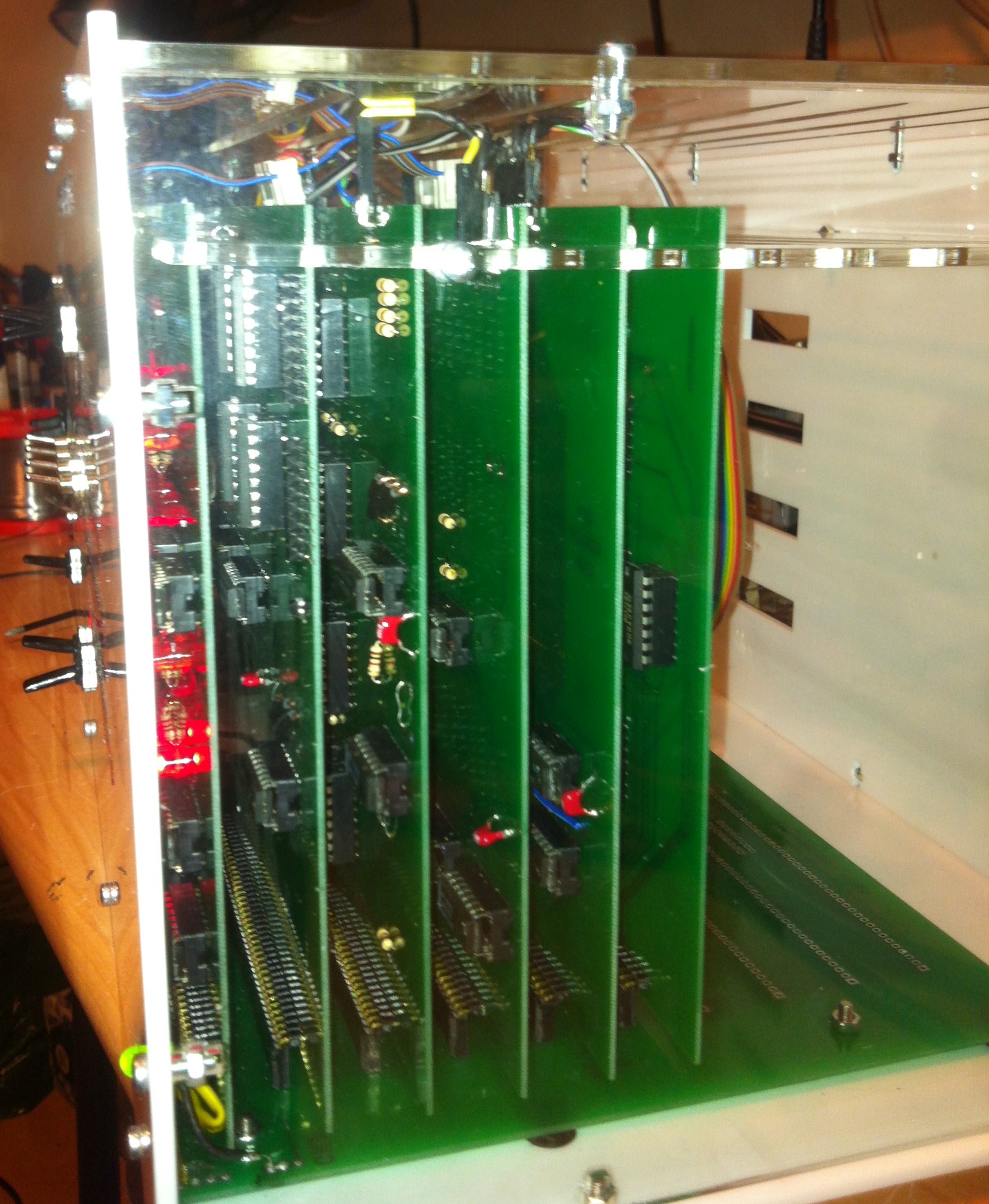
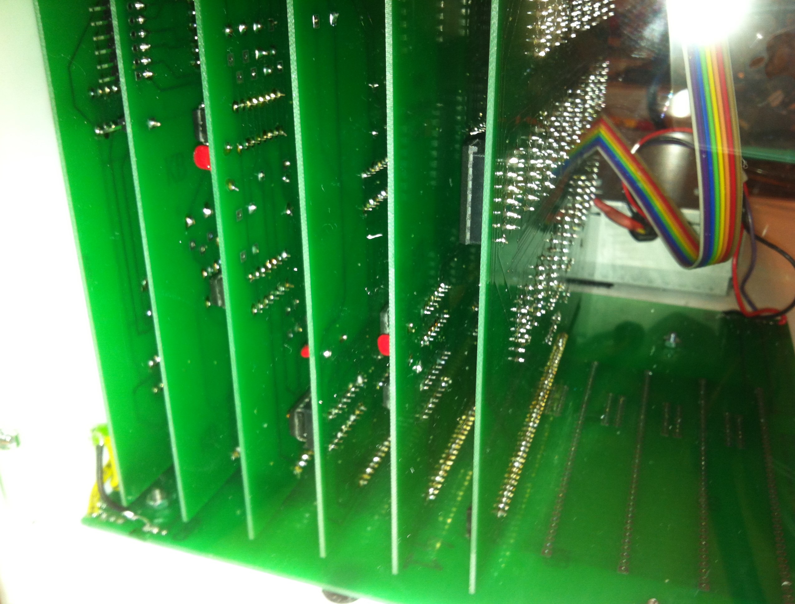
When I received the PCB’s the easy task of soldering them together could begin. It took me some time to finish them all. I first soldered all the IC sockets and then soldered the rest of the components. After that it was just a case of putting the right I.C. In the right socket and after a lot of checking and double checking the mark-8 PCB’s where finished.
The six finished MARK-8 PCB’s in pictures: (click on pictures for larger view)
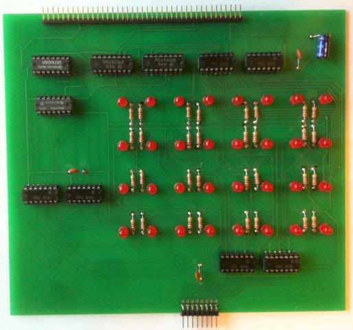
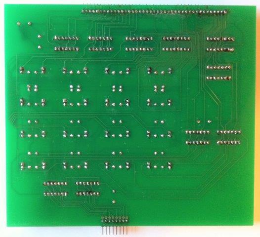
Above MARK-8 LED REGISTER DISPLAY board


Above MARK-8 OUTPUT LATCH BOARD front and back


Above MARK-8 1K MEMORY BOARD front and back. Shows the wire connections settings for 1K leftside beneath horizontal I.C.’s. See also in the documentation below this article.


Above MARK-8 ADDRESS LATCH board front and back


Above MARK-8 INPUT MULTIPLEXER BOARD front and back


Above MARK-8 CPU board front and back
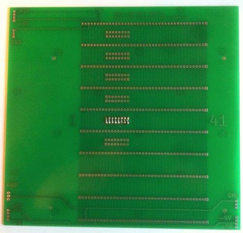
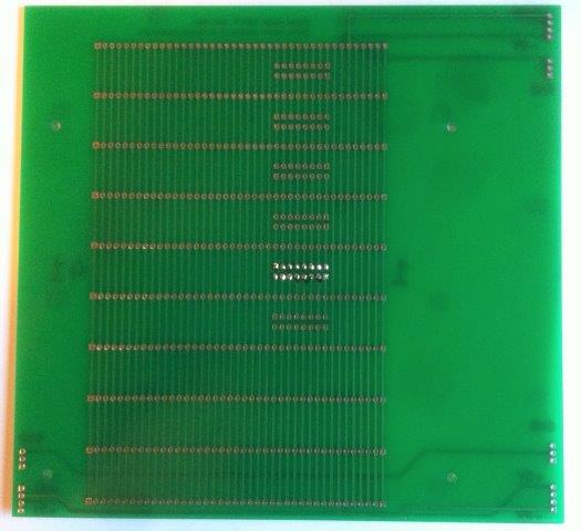
Above BACKPLANE BOARD back front and back. Notice the solderbridges see text.
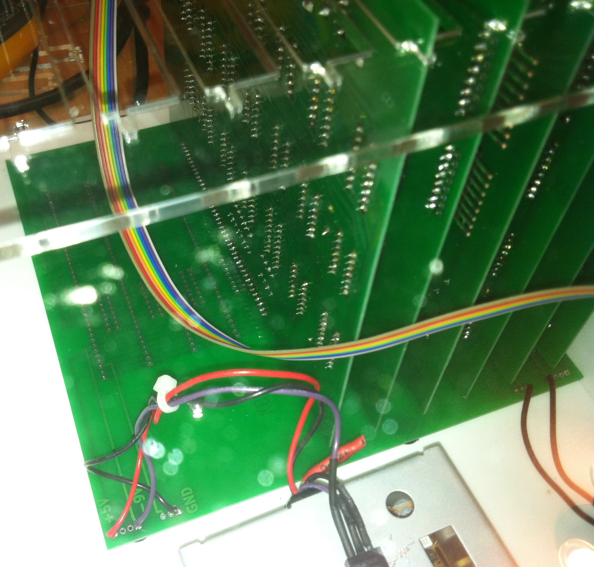
 As you can see in the pictures the boards all have a simple connector. The original MARK-8 had no connectors. You had to solder a wire from back through front and solder the boards together. So if there was a problem you had a hard time getting to the faulty spot. So thats why I decided to make an extra backplane PCB but at the same time keeping the 41 board connections exactly like the original. I could have used more robust connectors but with a little extra backup from a bracket (more on that later) the connectors are doing fine. It is also a very cheap way to connect the boards.
The only problem was the 41 pins. A connector with 41 pins is nowhere to be seen so I made them by placing two connectors on the PCB and the backplane side by side with (only on the backplane) a bit of glue to keep them lined out.
You also may notice on the backplane the extra rows of 2 x 8 solder holes. This was not mentioned in the original article but some tracks had to be cut between the INPUT MULTIPLEXER and the ADDRESS LATCH board but remember that you have to make the connection with wirebridges on the backplane between the INPUT MULTIPLEXER and the CPU board because they are connected with all 41 tracks. The backplane has also room for 4 more boards for future expansions like extra memory or maybe a self designed circuit like an eprom board ;-).
Now that I had the PCB’s ready I had to make the front panel, Because the MARK-8 uses switches as an input device (no not a keyboard). The output is the LED board (No not a monitor). Without a front panel you cannot test the MARK-8.
I made  a layout in Coral Draw for a complete enclosure with a front panel which took me some time and some versions befor
 e I got the one which suited me most. (You can find the final files for the enclosure at the bottom of this page.) I also made a bracket for the PCB’s to hold them straight in place with the backplane. The complete enclosure is put together with M3 screws 12mm long. Just use 3mm acrylic and a laser cutter to make the enclosure. All you have to add yourself is 4 holes in the bottom to fasten the backplane to the bottom after you lined out the LED board with the front panel. As you can see in the pictures I also glued in some strips of red acrylic because I did not like the open space to the PCB. And be honest it just looks nice doesn’t it?

BRACKET TO HOLD PCB”S NICE AND TIGHT IN PLACE.
For the DATA ADDRESS switches I used 8 switches with a long handle SPDT (Single pole Double throw) I used the same switches as Power switch and run/step and JAM switch. For the other switches I used six momentary switches SPDT. The Switches for the HIGH/LOW ADDRESS are a bit bigger because I had the laying around and liked them 😉

MARK-8 computer one of the 11 on/off switches

MARK-8 computer one of the 2 momentary switches

MARK-8 computer one of the 4 momentary switches
A very very big help was the document from Bryan K. Blackburn which explains how all the wires are connected to the PCB’s. You will find it at the bottom of this article for download. All in all I think if it wasn’t for that great website of Bryan I doubt if would have been as successful with this design as I was.
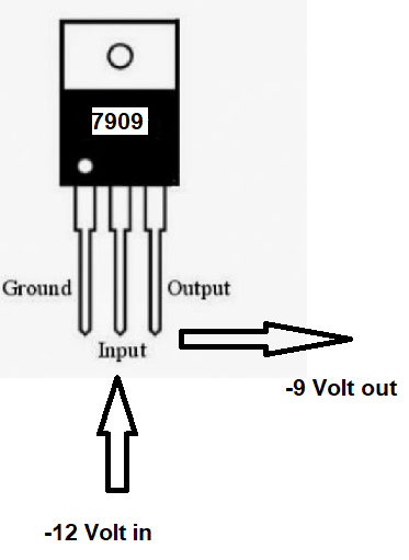 After a lot of soldering I only needed a power supply. The MARK-8 needs +5Volts and -9 Volts (-9V for the 8008 cpu). So I used an old PC power supply which provides +5 volts but not -9 Volts only -12Volts. But that is easy I just used an 7909 negative power regulator on the -12 Volts line of the PC power supply and there you go. All power connections go through the backplane and the power switch.
After I finished the construction I did not expect that the MARK-8 would run at the first time because you always make a small mistake don’t you? So I switched the MARK-8 on and I followed the instructions in the documentation to see if it worked as expected. And I could not believe my luck when everything worked in one go. Not one mistake was made and the whole thing worked the first time after months of hard work. See the video below to see the nearly finished MARK-8 in action. Only have to add the power LED right below and connect the power switch for easy ON/OFF. Also the Power supply is not fitted yet and is just hanging inside.
In the documentation is an example for a test program but I have a shorter one that has the same effect for testing. A led counter as seen on the video above.
Steps to take:
- Power ON
- All Data/Addrress switches on zero position
- RUN/STEP switch on STEP
- JAM switch on JAM
- Press down High load address (all leds out)
- Press down LOW load addres (all leds out)
- enter the following:
- 020 > press deposit
- 110 > press deposit
- 000 > press deposit
- 000 > press deposit
- 010 > press deposit
- 301 > press deposit
- 121 > press deposit
- 005 > press deposit
- Set JAM switch off
- Press interrupt switch
- Set RUN/STEP switch to run
- The computer start flashing leds.
- Finish
In the documentation the octal system is explained and also how to set a number for input into the MARK-8 computer. Here a short explanation. The eight Data/Address switches are divided into three parts like this 00 000 000. Each position has a value 21 421 421. So if you want to enter the numer 005 you set the eight switches to positions 00 000 101. A value of 201 is 10 000 001 and as a last example 310 is 11 001 000.
Don’t see the logic yet? Look at the switch settings for 310. The first 2 switches are set to 1. The value of the first switch is 2 and the second switch 1, together 3. At the next 3 numbers only the last switch is 1 with a value of 1. In the last section all switches are set to 0 so together you have 310. It’s that easy.
Some detailed pictures from the MARK-8 minicomputer project:

MARK-8 1K memory board close up

MARK-8 computer with experimental backplane

A look inside the MARK-8 computer while I am still working on it.

Detail of MARK-8 computer PCB connection with experimental backplane. I later made a professional one.
Below some pictures taken from the side of the clear acrylic housing,
If you want to make your own MARK-8 mini computer you can order download the PCB gerbers (see below) to make your own boards. A set of 6 MARK-8 PCB’s and 1 Backplane PCB (7 in total). Remember that the boards have all the errors and bugs removed which where present in the original so it is much easier to make a working MARK-8 with my replica PCB’s. If you have all the needed parts and follow the tips I gave above, then there is no way anybody can stop you having your own MARK-8 minicomputer. That is if you know what you are doing. Remember this is not a project for the novice.
MAKE YOUR OWN MARK 8 COMPUTER
Now available:
- The complete set of seven PCB’s including the backplane for building a MARK 8 are sold out but I have made the gerber files available for anyone who want to order the PCB’s at a PCB manufacturer. But beware only for yourself so not for commercial use or sale.
- Download gerber Mark 8 complete
Please make a small donation for the use of the free Mark 8 gerberfiles and the info on my webpage. You can do this with the paypal button here below on the left. Thank You.

Budgetronics can supply you with the difficult to get 1101 memory IC’s see.
The prices you see on Budgetronics include 21% VAT but if you order from outside the EU prices will be automaticly reduced with 21% VAT at checkout. Shipping costs will be calculated at checkout and can be viewed before finishing your order.
Resources:
http://www.bytecollector.com/mark_8.htm Great documented website about the Mark 8. I have taken some documents from this site which helped me a lot during the succesful construction of the MARK-8.
Download: (right click and choose Save as)
Coral draw files MARK-8 enclosure
MARK-8 construction documentation (from website Bryan Blackburn)
MARK-8 front panel construction (made by Bryan Blackburn)
MARK-8 bugs list (The PCB’s I made have the bugs corrected so you do not have to worry about that.)
Original hand drawn MARK 8 circuits design by John Titus (Provided by Andrew Davies)
UPDATE:
Dick Jugel made two MARK 8 mini computers with my boards and he has written an Arduino sketch to serve as a kind of BIOS and drive the control panel with virtual switches – it uses a Mega 2560 Arduino to SD Card storage for programs and data. So you do not have to make a switchboard and can control the MARK 8 with an Arduino. Here you can download this sketch as a ZIP file
Dick also made a video about his build with the PCB’s he ordered from me:
And another video of the MARK 8 with the PCB’s I made.